SMT Line
Dossier produced with the invaluable and attentive help of Thibault Lestavel, engineer at Kickmaker.
In this dossier, you’ll discover what goes to make up an SMT (= Surface Mount Technology) assembly line, which is a production method for printed circuit boards – and by extension, a process applicable to the assembly of a mainly electronic product. Here, you’ll discover the different stages that make up this method, and the technologies employed. This example is intended to be general in nature, and should not be regarded as the only way of doing things.
Enjoy your reading!
Contents
Entrance control and storage
Assembly Line PCB & SMT
Assembly and functional tests
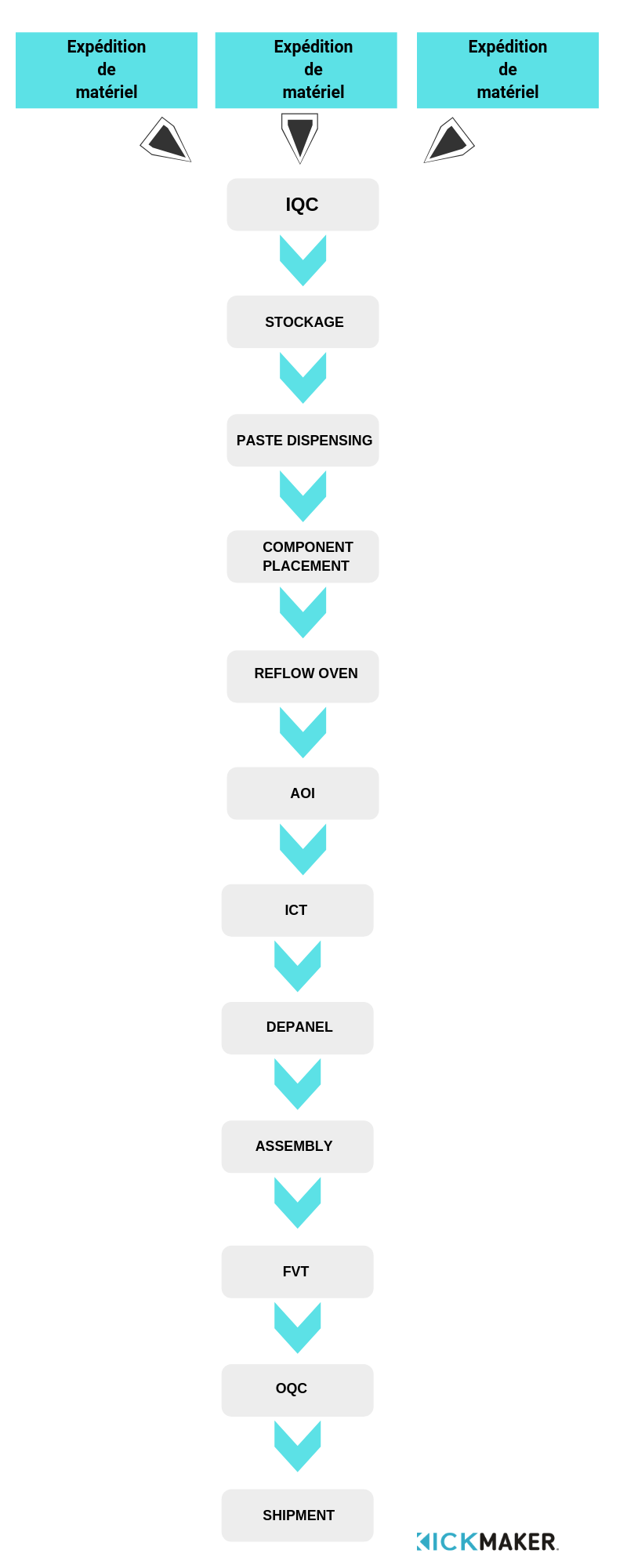
Material shipment, IQC & storage
Equipment can be shipped directly to EMS from a number of suppliers. This includes in particular :
- electronic components (resistors, capacitors, integrated circuits, connectors, etc.) ;
- mechanical components (plastic parts, screws, etc.);
- other types of components (batteries, motors, glue, etc.).
The packaging of these components must remain functional, both to guarantee storage quality and to maintain productivity. Although storage costs are calculated on the basis of gross packaging volume, it is important to bear in mind the trade-off between optimizing packaging on the production line (winding, individual boxes, etc.) and that required for storage (e.g. large stock boxes).
This must be taken into account at the start of the project, when considering how the product will be assembled, so as not to have to change the type of packaging in the factory.
IQC (incoming quality control)
These components undergo an input quality control (IQC) to ensure that they meet both customer and EMS criteria in terms of aesthetics, packaging, etc…
IQC can also include basic functional testing, as well as selective sampling checks, again to ensure that the component meets design tolerances.
Although sampling is often part of EMS best practice, it is also important to define quality control criteria according to the criticality of the design and the level of confidence in suppliers.
For example, if variability is noted in prototype batches from a newly qualified supplier, it may be worth adding a special check for the first few months of production, to ensure that variability problems are now under control. These control steps should be specified in terms of duration and sampling rate. Overqualification, i.e. too many inspection criteria for a large number of samples, will inevitably lead to higher costs.
Storage
Before being stored, incoming goods are re-labeled and scanned to match the plant’s ERP and ensure proper traceability.
Storage must be carried out under the right conditions, taking into account the specifications of the various components. For example, electronic components often require temperature and humidity control. This applies even more so to chemical compounds such as glue, solder paste etc. In addition to temperature and humidity controls, these components also require a chemically controlled environment and have a use-by date.
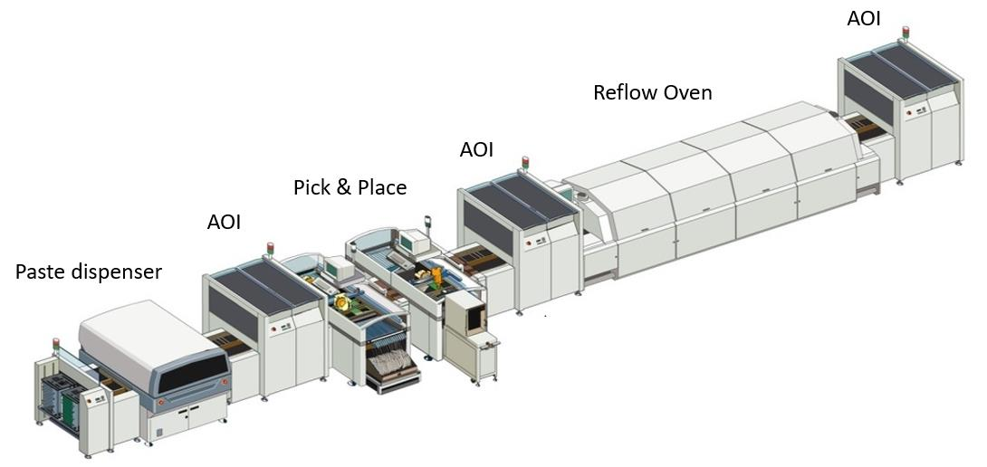
Assembly line PCB & SMT
Paste dispenser
As the printed circuit board is considered here as an external manufactured element, it undergoes the process described in the previous section.
The PCB’s journey begins with the deposition of solder paste, a tin-based chemical that melts in the reflow oven to create the solder joints. The choice of solder paste is critical, and must match the thermal profiles of the reflow oven. Incorrect solder paste selection can result in poor quality solder joints, such as dry soldering or the appearance of air bubbles.
These assembly problems are usually not detectable by optical or functional testers, but can be found under X-ray or other destructive quality control procedures. It is therefore important to carry out quality control sampling, both at the start of the process to ensure that it is under control, and during production.
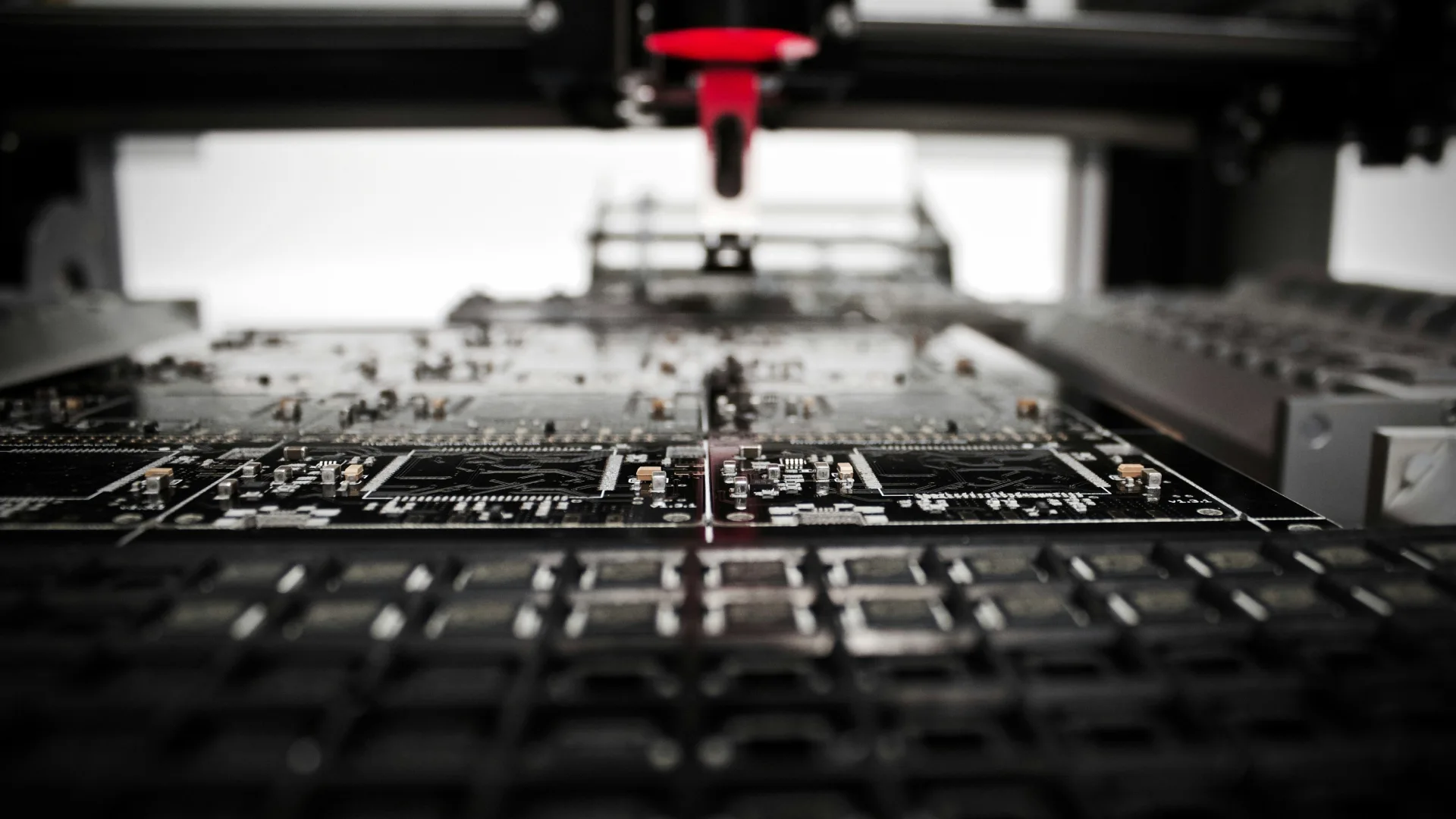
Once the solder paste has been deposited, the conveyor stops at the pick-and-place machine. A robotic arm picks up the electronic components from various coils and deposits them on the PCB footprints. This machine can deposit up to 50,000 components per hour!
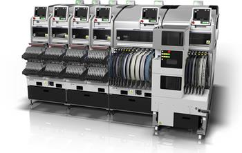
Pick and place machine
On the assembly line, the EMS often places several pick-and-place machines to manage the number and type of different part numbers to be fitted.
For example, a pick-and-place machine for resistors/capacitors needs to have a high throughput rate, while a machine for connectors needs to be able to lift “heavy” components at a lower throughput rate, due to the limited number of such components.
What counts for the EMS (and has a direct impact on manufacturing costs) is bottleneck management. For example, production runs smoothly if cycle times are uniform at each station. But this is rarely the case. Some stations have variable cycle times. This problem can be managed by using intermediate storage stages, increasing the number of stations, modernizing machines, etc.
Reflow oven
The reflow oven consists of an oven equipped with a conveyor to follow a defined thermal profile. SMT lines are not usually dedicated to a single project. Oven thermal profiles depend on the PCB, components, solder paste, etc. It’s important that when the line is set up, the quality department checks that all parameters are correctly entered into the machine before the line starts running. These checks should be documented in a “Go For Prod” checklist

Profil thermique du four à refusion
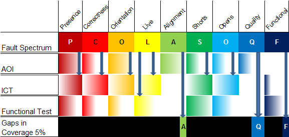
Automated Inspection Control (AOI)
Most of the time, these AOI machines are used at different stages of the SMT line. AOI machines can be placed after each step (paste distribution, pick and place, reflow…) but as all this comes at a cost (time and material) compromises have to be made regarding bottleneck, production time, machine capacity, scrap target, etc. Nowadays, AOI machines are so efficient that they can detect misalignments down to the micrometer, check 3D parameters of welds, component orientation, and so on. At the start of production, these machines need to be parameterized and even “trained” to filter out false positives.
The placement of components must take these optical inspections into account. Large components should not be placed next to very small ones. Otherwise, optical coverage would be reduced and the PCB would not benefit from the advantages of this powerful tool.
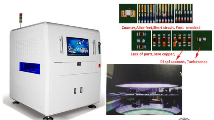
Machine AOI et quelques problèmes détectés
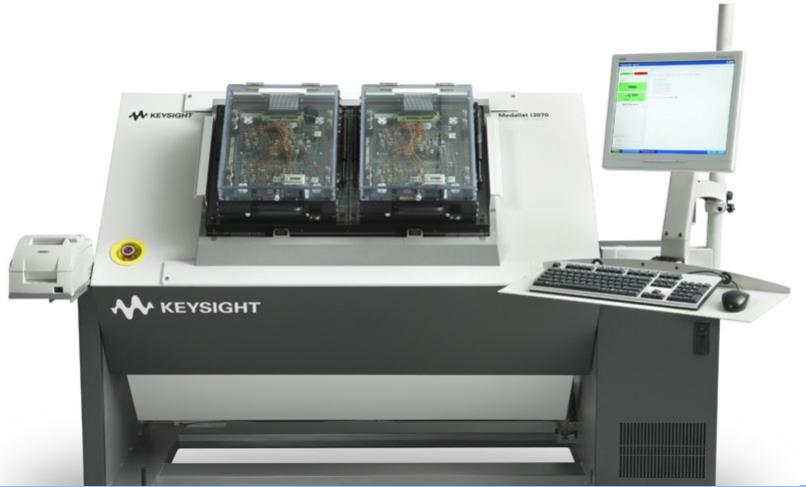
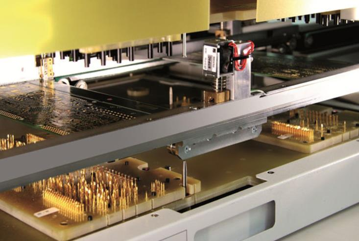
In-circuit tester (ICT)
Imagine an ultra-fast multiplexed multimeter capable of measuring both passive and active components. Add power testing and programming capabilities, and you get the ICT.
The ICT can be used to check certain characteristics of a component, such as its orientation, its presence, whether it is open or short-circuited; or to carry out diode tests of integrated circuit inputs/outputs. It’s also possible to check power supply rails, board consumption, perform boundary scans or even program an integrated circuit.
The ICT principle is based on the physical contact of a nail bed with the board’s signals via test points. It is therefore very important to add as many test points as the design allows, especially when ICT is required: it’s a powerful tool for checking that component values are within the tolerated range. Note that ICT provides test coverage based on component testability. The test coverage rate is calculated according to the type of components tested and the possibility of making these measurements.
Let’s take the example of a board with a 100 nanoFarads capacitor. If you have test points on both sides of the capacitor, you can test its presence, its value, whether it’s open-circuited or short-circuited.
Let’s take the same example, but add a 10microFarad capacitor in parallel. It will only be possible to carry out the presence and value test on the 10microFarad capacitor, as the 100 nanoFarad would fall within the tolerance of the higher-value capacitor.
ICTs are often used on panelized PCB assemblies to reduce cumulative test time.
Depending on the complexity of the board, the ICT cycle time can be quite long (several tens of seconds) and become the bottleneck of the line. What’s more, the ICT machine is costly and irrelevant for all designs, so it’s important to arbitrate by specifying the need, the number of tests required and the complexity, application and final cost of PCB assembly.
Depanel
Depanel is the mechanical process of separating each printed circuit board from its panel. Many processes exist, most of them mechanical, and some of them can damage the components present on the printed circuit boards. Indeed, depaneling can create mechanical stresses on printed circuit boards (e.g. bending) which can damage surrounding components. This is also why it is recommended to leave space between the edges of printed circuit boards, or even to carry out stress measurements when criticality demands it (common practice in the automotive industry).
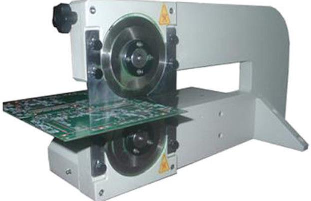
V-cut PCB depanelizer
Assembly & functional tests
While the preceding steps are generally carried out in the same order, assembly and functional testing are highly dependent on the design of the final product and the expected quality. It is possible to verify each assembly step using functional validation tests (FVT), cameras or an operator; or to carry out only one final test once the product has been assembled. The balance between test time (and therefore cost) and quality objective must be determined according to the product and its application.
For example, the “cost of quality” for an automobile compared to a generic consumer good will be drastically different, as an assembly defect will not have the same criticality for the end customer.
Assembly process
Once depaneling is complete, printed circuit boards can be assembled in their final mechanical enclosures. This is often done with the aid of assembly jigs, which help to ensure that assembly methods are appropriate and meet designers’ requirements. A good practice is to “detrend” the design to ensure that under no circumstances can components be assembled in the wrong direction. For example, an asymmetrical centering pin can be added to the PCB corresponding to the mechanical housing. These precautions should not prevent the designer from specifying possible errors or even reject criteria.
Most assembly work is carried out by unskilled operators who have no knowledge of the final product and its design constraints. We therefore need to put ourselves in the same position, and ask untrained people to assemble the product when setting up the line, by analyzing their gestures and reactions when reading the assembly document. It will then be possible to observe behaviour that is difficult to predict, to understand certain difficulties and to draw from them better practices, an update of the assembly guides or even an update of the design.
Trying to make mistakes (without doing anything unnatural) on each of the assembly steps is also a good way of checking whether the right tools are being used, whether the jig is strong enough to withstand poor handling, and whether the process is robust enough to detect poor assembly afterwards.
FVT (functional validation tests)
As mentioned above, functional validation tests (FVTs) are used to test the product during the various stages of assembly. The purpose of FVTs is to test the product’s various functions and validate their operation. Examples of functional tests include button-press simulation and display testing, as well as electronic tests such as checking supply voltages, communication bus checks, etc.
It’s a common mistake to want to qualify a product rather than validate it functionally. Qualification (design margin, checks on behavior within specification limits, etc.) is carried out at the design stage, not during production. Performing qualification during production would result in a high scrap rate, due to the narrow limits set for a large number of criteria. This over-qualification would lead to significant additional costs.
Over-quality is just as dangerous as under-quality. It can drastically increase the final price of the product, as well as the burden on quality teams who will end up needing a disproportionate amount of technical support.Assembly line and FVT evaluation can be carried out using quality processes such as GR&R (Gauge Repeatability & Reproducibility). An example of this standardized test is to assemble 30 different products on each station with 3 untrained operators, measure success/failure ratios and use a few statistical formulas to determine the efficiency of the process implemented.
This process is completed by the use of “black samples” (or “silver samples”) and “golden samples”. These samples are prepared by R&D for each station. The “golden sample” is an R&D sample considered as a functional reference against which other products can be compared.
The “black samples”, also prepared by R&D, have known defects which must be detected by FVT test benches or quality control stations.
Once again, a balance must be struck between the criticality of the function and the time invested in testing it. Be sure to take into account the development required for this type of detection, which can sometimes exceed several tens of thousands of euros in R&D and the same amount in equipment.
In addition, the FVT provides a coverage score which, when added to the ICT and AOI, gives the total coverage rate.
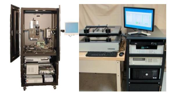
Functional Validation Testers (Left: TFT display tester, Right: PCBA functional tester)
Typical test coverage score
OQC & shipping
Once the product has been assembled, quality controls are put in place to ensure that production does not deviate from its initial objectives. These checks may include “out of the box” tests (user tests), aesthetic checks, etc.
For obvious reasons of cycle time, not all products can reach this level of inspection. In this case, sampling can be used to ensure consistent quality throughout the production process. Specific quality controls can be added as problems arise during the product life cycle. For example, extensive sampling at the start of the production life-cycle, then rationalized, systematic control of a single characteristic if it has led to regular customer complaints, etc.
The final stage of the process is shipping. As with incoming material, packaging is very important.
For example, the final packaging can be used if the product is ready to be shipped to the customer. But if the assembled product needs to be packaged with accessories (cables, chargers…) in a different location, or repackaged due to regional constraints, in this case the choice of intermediate packaging is more judicious.Packaging is important to ensure that the product will not be damaged during transport (by road, sea and/or cargo plane) and must take into account the different constraints of these modes of transport.
Last but not least, palletization must be taken into account to optimize shipping costs and facilitate worldwide shipment.
Tracability
We touched on some of the quality control processes and actions in the previous section. But quality engineers are not only responsible for ensuring compliance with good production and assembly practices, or for checking that quality remains stable over time. These traceability systems are fed by barcodes, test results or other feedback. The most advanced traceability systems require each individual step to be started and completed by a unique traceability action.
Take, for example, the assembly of a PCBA into a housing:
– Step 1: the operator scans the PCB’s QR code
– Step 2: the traceability system verifies that the PCB is “authorized” to participate in this assembly step. Indeed, an operator could have “skipped” a station. In this case, the ERP must reject the part, and a quality indicator is triggered.
– Step 3: the printed circuit board is “cleared”, and the operator can assemble the housing and PCBA.
– Step 4: the operator finishes assembly, takes another QR code and sticks it on the housing.
– Step 5: The operator scans this QR code. The sub-assembly is now in the system and ready for the next station.
This traceability system also enables inventory management, as well as the possibility of tracing the source of a problem detected later in the assembly process or by the end customer, and taking the necessary corrective action.
Glossary
ERP: “Enterprise Resource Planning”
EMS: “The term Electronic manufacturing services (EMS) is commonly used in the electronics industry to designate companies that provide subcontract manufacturing services for electronic products: printed circuit boards (PCBs), PCBAs (printed circuit board assembly, sub-assemblies). Customers are often referred to as OEMs. In addition, an EMS often offers design, validation, distribution and/or after-sales service. When the entire development process is subcontracted, it is referred to as ODM.
OQC: In printed circuit board manufacturing, quality control, or QC for short, is a process by which entities examine the quality of all factors involved in production. ISO 9000 defines quality control as “a part of quality management focused on meeting quality requirements”. Finished products must be inspected before delivery, known as OQC, outside quality control.